Mipox's polishing services for semiconductor-related wafers contribute to the development of new products and technologies. During the development process, development may be abandoned due to high equipment costs, time inefficiency, or difficulty proceeding with manufacturing and technology development from scratch.
In such cases, outsourcing the manufacturing process is one of the best options available, and Mipox’s polishing services can provide the best materials and equipment to suit your needs.
In this article, we will introduce the strong features of Mipox's polishing service for semiconductor wafer-related contract polishing and what kind of technology is used to process the materials.
目次
- Mipox Polishing Services
- Typical Applications for Semiconductor Related Wafers
- 1. Surface planarization and precision flat polishing of ceramics of polycrystalline materials and composite substrates.
- 2. Beveling and mirror edge processing of single crystal substrates for power devices (GaN and SiC)
- 3. Edge trimming process, to reduce the risk of cracking from wafer edges during thinning.
- Conclusion
- Mipox's Business
Mipox Polishing Services
Our polishing service is characterized by the following three major features.
- Most of materials required for the polishing materials and equipment are using in house, and an applicable to services polishing of customer requirements.
- The polishing process covers a wide range of products from semiconductor wafers to parts such as ornaments and metal rolling roll materials.
- The polishing process covers a wide range of products from semiconductor wafers to parts such as ornaments and metal rolling roll materials.
These characteristics are our major strength, and we are able to freely adjust and select abrasive materials and polishing equipment to meet our customers' requirements and achieve the best possible processing results.
For projects involving research and development, we have a system which is easily accepted by our customers, such as disclosing polishing processes (know-how), transferring technology including polishing equipment. Also, we are providing flexible support up to the start of mass production, depending on the progress of development (testing), prototyping, and mass production.
Typical Applications for Semiconductor Related Wafers
1. Surface planarization and precision flat polishing of ceramics of polycrystalline materials and composite substrates.
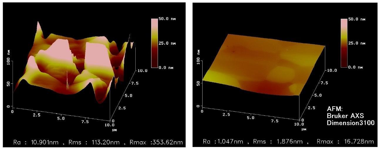
For polycrystalline ceramic materials and composite materials, typical materials include aluminum nitride, alumina ceramics, and polycrystalline SiC, which are generally considered to have limitations in improving the accuracy of plane polishing. However, we have established a processing method that enables us to obtain high-precision planes beyond the realm of ordinary polishing processes and apply it to our own polishing service.
In the precision flat surface polishing process for ceramics, the processing results strongly depend on the performance of the liquid abrasive. In order to obtain a good surface condition, it is necessary to precisely control for the distribution of an abrasive size. We are able to suit the object for the main ingredient in the slurry, such as their dispersion, concentration, and the mixing ratio of each material to be processed.
In order to apply for the latest technology, we are using knowledge through the development of polishing materials for HDDs. Slurry manufacturing technology is one of our strong points as well as our polishing film. Those knowledge can be apply to polishing service.
Our precision flat surface polishing process contributes to the creation of new applications for each material. For example, we have many achievements in new applications of SiC as a component for the heat sink function of power modules and high-functionality wafers used for high-power LED manufacturing.
2. Beveling and mirror edge processing of single crystal substrates for power devices (GaN and SiC)
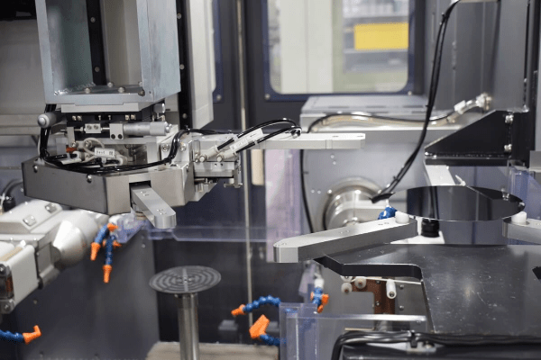
Our polishing service also includes edge processing, which is closely related to the planar polishing process, and we have developed and introduced our own specialized processing machines for power device single crystal substrate applications.
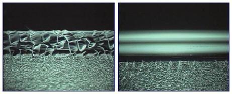
Edge mirror processing is common in the manufacturing process of single crystal silicon wafers, but for single crystal SiC and GaN substrates, it has been difficult to produce high quality edges with high yield and high efficiency due to their unique physical properties.
We have developed processing methods that mainly apply our own abrasives, especially "polishing films," and we have established processes for both beveling and mirror edging to solve the technical issues faced by single crystal SiC and GaN substrates.
Mirror-edging of single-crystal SiC and GaN wafers is effective in securing wafer strength and improving stability during surface polishing (edge dropout prevention). It has also been proven to be effective in suppressing defects during epitaxial layer formation and is one of the processes that have been attracting particular attention in recent years.
In addition, our polishing service is not only limited to standard round wafers, but also supports square wafers. Also, one of our strong points is providing to beveling processing for substrates after dicing.
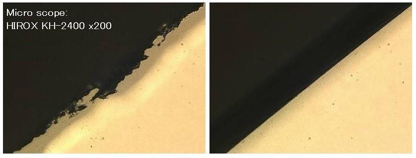
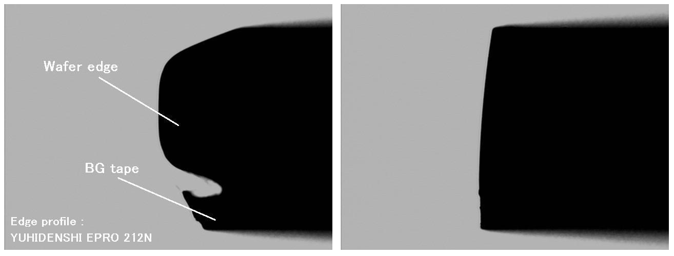
3. Edge trimming process, to reduce the risk of cracking from wafer edges during thinning.
The cross-section of the wafer edge is usually trapezoidal or R-shaped, but as the wafer is made thinner, it gradually becomes sharper and more susceptible to breakage.
Therefore, it is typical for numerous chippings and microcracks to occur during the thinning process of backside grinding, increasing the risk of wafer breakage. However, this risk can be significantly reduced by applying the edge trimming process in our contracted polishing service,
Edge trimming is the important for processes involving multilayer stacking, and it has a highly effective process for reducing the time required for the thin grinding process. We have achieved this process with our own unique method using our own polishing tape, and we offer it as a polishing service.
The process utilizes the advantages of the "similar method" to enable trimming while maintaining concentricity to the original wafer circumference.
Furthermore, even if the wafer is covered with protective tape (protective film), it can be processed without being affected by the tape. In addition to silicon wafers, this process is also applied to compound semiconductors (InP), which are easily damaged.
Conclusion
As mentioned above, we offer " polishing services" that cover a wide range of processing subjects (areas) using polishing processes completed by maximizing the use of our own polishing materials.
Although polishing processes become increasingly mechanized with specialized processing machines, it is a high proportion of the process still relies on know-how (experience). Therefore, we believe that there is a limit to how efficiently a customer can establish a good process in a short period of time by themselves.
In order to support and establish efficient processes for our customers, we have opened up the process technology including know-how that we have been accumulating in-house as our "polishing service". We hope that our " polishing service" will contribute to speed up the product development of each customer and be an effective breakthrough for developing new technologies.
Mipox's Business
We, Mipox Corporation, are a manufacturer of various abrasives, including our main products "polishing films, cleaning films, and liquid abrasives (slurry). We mainly manufacture abrasives for precision electronics applications and are expanding into the "contract business" by applying the abrasive manufacturing technology over many years.
In terms of business development, we provide each product and service to our customers. Polishing service is utilizing each polishing material product manufactured in-house also we have Service coating business which is using various to make a functional film based on customer requirement, this is our one of main business.