Introduction
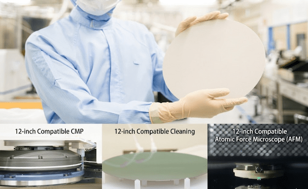
In March 2026, Mipox established a CMP processing line compatible with 12-inch (300mm) wafers and successfully commenced full-scale operations.
Against the backdrop of rapid advancements in AI and the digital society, alongside the widespread adoption of next-generation mobility, the demand for higher performance and manufacturing efficiency in semiconductor devices has been intensifying year after year.
In response to these market needs, Mipox has made a full-scale entry into the 12-inch CMP sector, leveraging our foundational ultra-precision polishing technologies. Furthermore, we are concurrently expanding our facilities for the "bonding process," aiming to establish a "Total Foundry Service" that seamlessly integrates everything from polishing to bonding.
This article provides an in-depth look at the unique strengths of Mipox’s CMP processing line and the strategic business advantages it offers to next-generation semiconductor manufacturing.
目次
- What is CMP? An Essential Technology for Achieving Nano-Level Planarization
- The Challenges of Planarization: Driven by 12-inch Wafers and 3D Packaging
- Mipox’s Unique Advantage: The Technological Fusion of "Coating, Cutting, and Polishing"
- Future Outlook: Expanding Bonding Processes and Contributing to 3D Integration
- Conclusion
What is CMP? An Essential Technology for Achieving Nano-Level Planarization
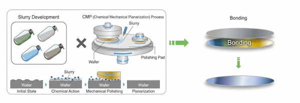
CMP (Chemical Mechanical Planarization) is a polishing technology that combines chemical and mechanical actions using polishing slurries and pads to achieve ultimate flatness on the wafer surface.
This technology enables the planarization of surfaces featuring a mixture of dissimilar materials and allows for nano-order precision control—challenges that were difficult to overcome with conventional polishing methods.
From advanced logic semiconductors to next-generation power devices, CMP technology is positioned as a fundamental process that underpins the manufacturing of all high-performance devices.
The Challenges of Planarization: Driven by 12-inch Wafers and 3D Packaging
As AI and next-generation mobility become increasingly prevalent, there is a growing demand for even smaller and faster semiconductor devices. Three-dimensional (3D) integration, such as TSV (Through-Silicon Via), has emerged as a key solution to these requirements; however, this approach demands a level of surface planarity that far exceeds the capabilities of conventional processes.
1.Risk of Bonding Failures
Even slight surface irregularities can lead to insufficient bonding strength during chip stacking, resulting in a significant decrease in yield.
2.Challenges in Large-Diameter Processing
With the transition to 12-inch wafers, advanced control technologies that ensure uniform polishing across the entire surface—extending to the outermost edges—have become indispensable.
Mipox’s Unique Advantage: The Technological Fusion of "Coating, Cutting, and Polishing"
The most significant characteristic of Mipox lies in the sophisticated fusion of our three core technologies: "Coating, Cutting, and Polishing." As a manufacturer-based foundry operating across three business segments—Abrasive Development and Manufacturing, Functional Coating, and Precision Polishing—we provide unique added value that sets us apart from the competition.
1.Optimized Processes with In-house Developed Slurries
Leveraging our expertise as an abrasive manufacturer, we develop proprietary slurries optimized for specific materials and target precision levels. Through our unique CMP processes, we achieve a balance between superior planarity and low-surface-damage.
2.Support for Diverse Advanced Materials
We provide broad support for processes requiring extremely high-level planarization, including Cu (copper) damascene projects, surface roughness improvement for bonding applications, and wafer manufacturing involving various functional materials.
3.Commencement of Contract Polishing Services for 12-inch SiC Wafers
SiC (silicon carbide), a focal point for next-generation power semiconductors, is rapidly transitioning to 12-inch diameters due to expanding demand in the EV and power infrastructure sectors. Building on our proven track record in proprietary polishing developed with 8-inch SiC wafers, Mipox has launched contract polishing services for 12-inch SiC wafers. We deliver streamlined and efficient manufacturing solutions.
| Category | Mipox's 12-inch CMP | General Contract Processing |
|---|---|---|
| Process Optimization | Material-specific optimization with in-house custom slurry |
Standard processing with general-purpose slurry |
| Supported Materials | SiC and Cu and other advanced materials | Primarily silicon |
| Integrated Capability | From polishing ➔ bonding end-to-end (Scheduled within FY2027 Q1) |
Polishing only (inter-process transport required) |
Future Outlook: Expanding Bonding Processes and Contributing to 3D Integration
Mipox is currently advancing the establishment of a 12-inch compatible bonding infrastructure, positioning it as the next strategic phase following our CMP processes.
Projected Completion: Within FY2026 (by March 2027)
Our integrated system, encompassing everything from polishing to bonding, will enable support for next-generation 3D integration utilizing Through-Silicon Via (TSV) technology.
The establishment of this end-to-end workflow will eliminate risks of contamination and damage associated with transport between processes, while simultaneously achieving significant reductions in logistics costs and management overhead.
Conclusion
With the full-scale operation of our 12-inch compatible CMP line, Mipox has further strengthened its technological foundation for cutting-edge semiconductor manufacturing. By fusing our core technologies of "Coating, Cutting, and Polishing," we go beyond simple contract processing to serve as a total foundry. From SiC and Cu solutions to upcoming bonding processes, we are committed to providing seamless support for our customers' innovations.
- CMP (Chemical Mechanical Planarization):
- A technology that combines chemical action from polishing slurry with physical abrasion to planarize surfaces at the nanometer level.
- TSV (Through-Silicon Via):
- A vertical electrical connection that passes through a silicon wafer. A key technology in 3D packaging that enables high-speed inter-chip transmission, lower power consumption, and miniaturization.
- SiC (Silicon Carbide):
- A next-generation power semiconductor material for EV and power infrastructure applications. Known for high breakdown voltage and low loss, with ongoing adoption of larger 12-inch wafer diameters.
For Further Details (News Release):
https://product.mipox.co.jp/news/20260312/
No,399